I Can Die Now. - Intel Fab Tour!
0 up · 0 down · 0 ratings
Promos
Receive a $25 credit for Ting Mobile today when you sign up at linus.ting.com Get 50% off on your annual Zoho CRM subscription at: lmg.gg Linus travels to Israel to get a tour an Intel Manufacturing Center known as Fab 28. This level of access is absolutely unprecedented. Discuss on the forum: linustechtips.com Learn more about Intel Transistor's: youtu.be ► GET MERCH: lttstore.com ► AFFILIATES, SPONSORS & REFERRALS: lmg.gg ► PODCAST GEAR: lmg.gg ► SUPPORT US ON FLOATPLANE: floatplane.com FOLLOW US --------------------------------------------------- Twitter: twitter.com Facebook: @LinusTech Instagram: @linustech TikTok: @linustech Twitch: twitch.tv MUSIC CREDIT --------------------------------------------------- Intro: Laszlo - Supernova Video Link: youtube.com iTunes Download Link: itunes.apple.com Artist Link: soundcloud.com Outro: Approaching Nirvana - Sugar High Video Link: youtube.com Listen on Spotify: spoti.fi Artist Link: youtube.com Intro animation by MBarek Abdelwassaa @mbarek_abdel Monitor And Keyboard by vadimmihalkevich / CC BY 4.0 geni.us Mechanical RGB Keyboard by BigBrotherECE / CC BY 4.0 geni.us Mouse Gamer free Model By Oscar Creativo / CC BY 4.0 geni.us CHAPTERS --------------------------------------------------- 0:00 Intro 0:54 The Basics 4:05 Suiting Up 5:44 Enter the Fab 7:13 Diffusion Land 8:42 HVAC 10:44 an F1 Pit Crew? 11:22 Dry Etching 12:20 Lithography 13:53 Planarization 14:26 AR Training 15:23 Polishing 17:00 Control Center 17:57 Fab 38 Construction 18:48 Things we didn't see 21:45 Outro
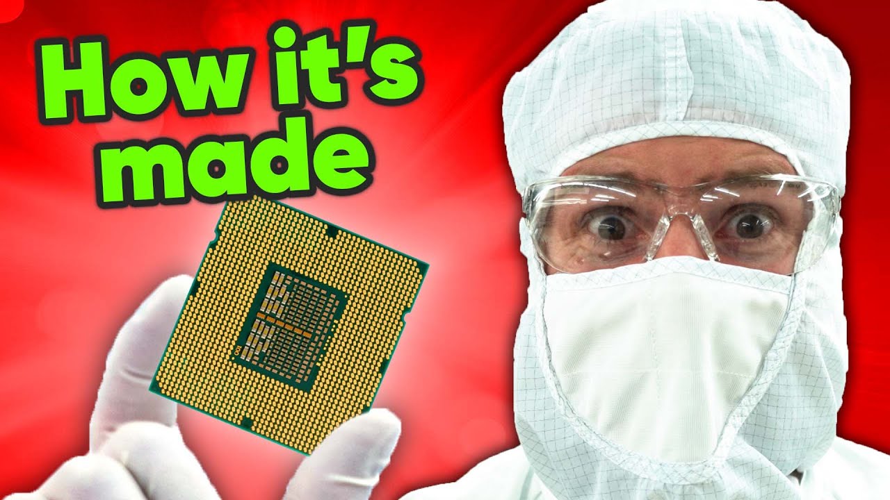
The Linus Tech Tips crew travels to Israel for an unprecedented tour of Intel Fab 28. The video opens with a candid setup of the trip, the host’s goal to visit a state of the art chip fabrication facility, and a nod to the significant costs and logistics behind making such a video. The narrator and guide introduce the basics of how CPUs begin as silicon ingots sliced into 300 millimeter wafers, emphasizing the edge management that keeps waste down and uniformity high. They then outline the core concept that billions of transistors and kilometers of wiring must be built with extreme precision, where even sub-nanometer contaminants can render a die defective. The segment highlights the high-level flow: start with silicon, perform ion implantation and diffusion to tailor electrical properties, then proceed through lithography to pattern billions of transistors with UV light through masks, followed by etching, planarization, and interconnect formation. This section emphasizes the scale, precision, and risks involved, setting the stage for deeper dives into each process area and the human elements behind a modern fab. The tour progresses into the human and procedural aspects of working in a fab. Viewers get the “suit up” sequence, including cleanroom garb and the importance of negative and positive pressure environments to keep particulates out. The crew moves from gowning to the main production floors, where robots and foups (containers holding silicon wafers) shuttle hundreds of dies through multiple stations. The host discusses the concept of a FOU P and how wafers are sorted for quality and categorized into processor families, such as core I7 and I9, after functional tests. The video frames the workflow as a well-coordinated pit crew operation, where maintenance tools are pre-arranged and downtime is costly. A recurring theme is the blend of cutting edge science with meticulous, almost ritualistic safety and cleanliness practices that enable reliable semiconductor manufacturing. As the narrative dives into specific processes, the audience is guided through diffusion land, deposition, lithography, and both dry and wet etching. The team explains how furnace-like diffusion steps introduce materials and how precise gas chemistries alter wafer surfaces. The lithography segment shows the photoresist coating, UV exposure through masks, and the rinse-and-repeat nature of patterning across billions of transistors. The tour then shifts to the deposition area where ultra-thin layers are added, and to the planarization and polishing steps where even atom-scale removal must be controlled. Throughout, the host notes the staggering investment in equipment, costs per machine, the multi-layer structure of the fab, and the layered airflow architecture that maintains a pristine environment in which nanometer-scale features are created. A notable portion of the video focuses on training, remote assistance, and augmented reality tools used to maintain and operate the fabs. AR is highlighted as a practical solution for COVID restrictions, remote guidance, and hands-on training for maintenance, enabling technicians to visualize schematics overlaid onto real components. The host also shares insights into inspection and end-of-line testing, binning, and the post-wafer steps such as packaging and burn-in to validate aging characteristics. The larger strategic context is introduced with Intel’s IDM 2.0 plan and the ambitious Fab 38 expansion, intended to double capacity and weave new generation fabrication into the existing ecosystem. The video concludes with a reflection on the opportunity, gratitude to the Intel team, and a tease for future tours and continued sponsorships while also acknowledging the broader global chip shortage and industry dynamics. Overall, the tour blends awe at the technology with practical explanations of how the equipment and processes come together to create modern CPUs. It balances accessible explanations for non-experts with enough technical color for enthusiasts to appreciate the complexity and cost. The narrative underscores that manufacturing is as much about process discipline and logistics as it is about chemistry and physics. By the end, viewers are left with a sense of the scale of Intel’s expansion, the importance of relentless quality control, and the ongoing evolution of semiconductor packaging and manufacturing strategies. The video leaves room for further exploration of related topics such as bezel-free precision, advanced packaging, and the global implications of IDM 2.0 on the broader tech supply chain.
Topics · technology · manufacturing · science_and_tech · education · industrial_and_responsible_practices
Questions answered
- What is the basic flow of semiconductor fabrication at Fab 28?
- The basic flow starts with silicon wafers, followed by ion implantation and diffusion to tailor electrical properties, then lithography to pattern transistors, followed by etching and planarization to create interconnects, and finally deposition, polishing, and packaging steps before testing and binning.
- Why is AR used in the fab tour, and what benefits does it offer?
- AR is used for remote assistance, training, and overlaying schematics onto real equipment, enabling experts to guide on-site technicians without being physically present, which is especially valuable during COVID restrictions and for complex maintenance.