They're STACKING CPUs Now!
0 up · 0 down · 0 ratings
Promos
Start your build today at buildredux.com Lean about die stacking, and when it might show up in your next PC. Leave a reply with your requests for future episodes, or tweet them here: twitter.com ►GET MERCH: lttstore.com ►SUPPORT US ON FLOATPLANE: floatplane.com ►LTX EXPO: ltxexpo.com AFFILIATES & REFERRALS --------------------------------------------------- ►Affiliates, Sponsors & Referrals: lmg.gg ►Private Internet Access VPN: lmg.gg ►MK Keyboards: lmg.gg ►Nerd or Die Stream Overlays: lmg.gg ►Official Game Store: nexus.gg ►Amazon Prime: lmg.gg ►Audible Free Trial: lmg.gg ►Our Gear on Amazon: geni.us FOLLOW US ELSEWHERE --------------------------------------------------- Twitter: twitter.com Facebook: @LinusTech Instagram: @linustech Twitch: twitch.tv FOLLOW OUR OTHER CHANNELS --------------------------------------------------- Linus Tech Tips: lmg.gg Mac Address: lmg.gg TechLinked: lmg.gg ShortCircuit: lmg.gg LMG Clips: lmg.gg Channel Super Fun: lmg.gg Carpool Critics: lmg.gg
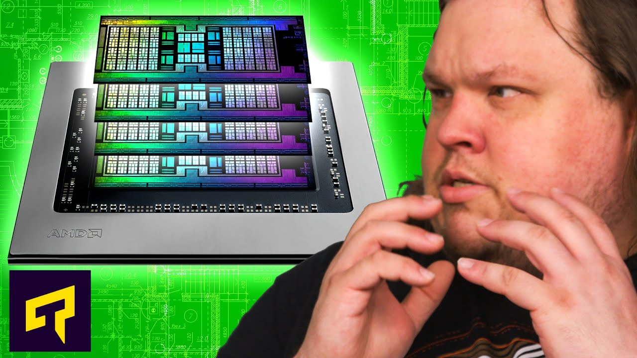
In this video, the host explains the concept of die stacking in CPUs, clarifying that this is not about stacking entire CPUs on a motherboard but stacking actual silicon dies within a package to add functionality. The discussion begins by contrasting die stacking in storage with CPUs, noting that Intel and AMD are pursuing different architectures to implement this technology. The segment on Intel introduces Foveros, a 3D stacking approach used in Lakefield that places a base die with support logic beneath a compute die containing the cores, connected by tiny micro bumps that are about half the width of a human hair. The video explains why close die-to-die communication is beneficial, including lower latency and improved power efficiency due to reduced data transfer energy. The AMD angle focuses on widening cache within the CPU package using 3D design, employing through-silicon vias (TSVs) to connect cache layers rather than micro bumps, which AMD claims can enable substantial performance gains. The host highlights the cache advancements, noting that a multi-core setup could reach up to 192 MB of L3 cache across two chiplets, with potential FPS improvements in gaming cited by AMD. The discussion ends with reflections on the future of high-resolution gaming and the possibility of even more integrated and cooler 3D CPU designs, along with a plug for Redux for custom PC builds and a reminder to subscribe for future episodes.
Topics · Technology · Computer Hardware · Semiconductors · Innovation
Questions answered
- What is die stacking in CPUs and how does it differ from simply stacking CPUs on a motherboard?
- Die stacking places multiple silicon dies within a single CPU package and connects them to enable faster communication and potentially better performance and power efficiency, unlike placing separate dies side by side on the same 2D surface.
- What is Foveros and how does Intel implement it in its CPU designs?
- Foveros is Intel's 3D stacking method where a base die containing support logic sits beneath a compute die with the cores, connected by micro bumps to enable tight integration and reduced interconnect distances.
- What is TSV and why is AMD using it for its stacked cache design?
- TSV stands for through-silicon vias, copper connections that pass through silicon layers to connect stacked cache layers, allowing more cache per chiplet and potential performance gains due to higher bandwidth.