The BIGGEST CPU Ever! - Waferscale Explained
0 up · 0 down · 0 ratings
Promos
Check out what you can fix with iFixit at ifixit.com There's a CPU out there as big as your head... Leave a reply with your requests for future episodes, or tweet them here: twitter.com ►GET MERCH: lttstore.com ►SUPPORT US ON FLOATPLANE: floatplane.com ►LTX EXPO: ltxexpo.com AFFILIATES & REFERRALS --------------------------------------------------- ►Affiliates, Sponsors & Referrals: lmg.gg ►Private Internet Access VPN: lmg.gg ►MK Keyboards: lmg.gg ►Secretlabs Gaming Chairs: lmg.gg ►Nerd or Die Stream Overlays: lmg.gg ►Green Man Gaming lmg.gg ►Amazon Prime: lmg.gg ►Audible Free Trial: lmg.gg ►Our Gear on Amazon: geni.us FOLLOW US ELSEWHERE --------------------------------------------------- Twitter: twitter.com Facebook: @LinusTech Instagram: @linustech Twitch: twitch.tv FOLLOW OUR OTHER CHANNELS --------------------------------------------------- Linus Tech Tips: lmg.gg Mac Address: lmg.gg TechLinked: lmg.gg ShortCircuit: lmg.gg LMG Clips: lmg.gg Channel Super Fun: lmg.gg Carpool Critics: lmg.gg
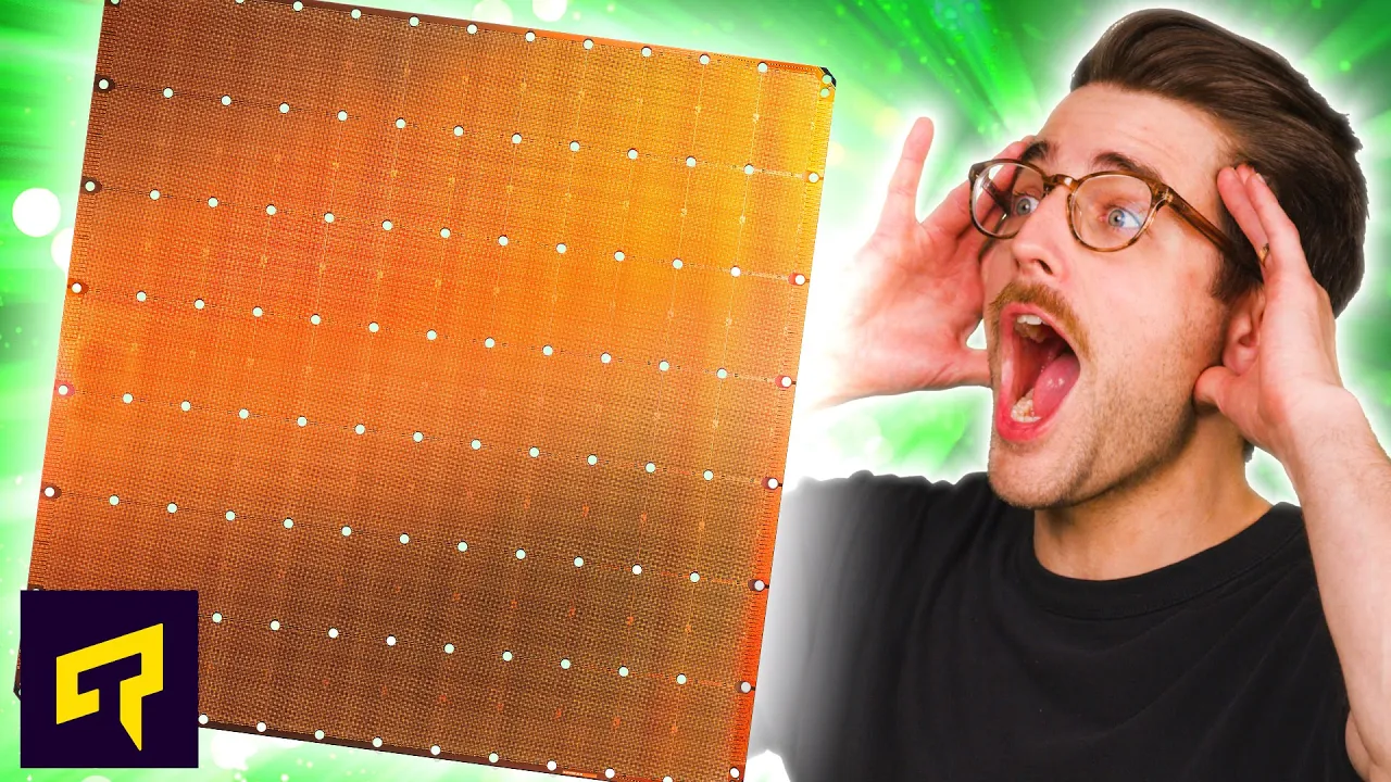
The video explains the concept of waferscale computing by examining Cerebras wafer scale engine 2, the largest chip currently in existence. It describes how traditional transistors shrinkage is offset by building an enormous single chip rather than many small chips, to reduce data interconnect latency and increase processing efficiency for AI and scientific workloads. The speaker notes that WSE-2 is built on a seven nanometer process and packs around 850,000 cores, spanning roughly 21.5 centimeters in length, which is more total area than multiple desktop CPUs combined. Because of its massive size and transistors, the device consumes about 15 kilowatts, implying that even a hypothetical PC integration would require substantial power infrastructure. The discussion covers the trade-offs between monolithic, wafer-scale designs and chiplet approaches, explaining that in some scenarios a single large chip can outperform a matrix of smaller chips with slower interconnects. The video also mentions memory constraints and the need for high-speed memory in such systems, comparing approaches like chiplets with large memory to a single monolithic wafer-scale design. Finally, the host connects these ideas to industry trends and echoes a continued interest in large-scale silicon for AI, while noting potential hurdles like manufacturing yield and cooling requirements. The segment wraps by highlighting the ongoing appeal of supersizing compute for data centers and AI research, and invites viewers to share ideas for future topics and subscribe for more content.
Topics · technology · computing · semiconductors · artificial_intelligence · data_centers
Questions answered
- What is the Cerebras wafer scale engine 2 (WSE-2) and how large is it?
- The WSE-2 is a single massive chip built on a seven nanometer process that contains about 850,000 cores and spans roughly 21.5 centimeters in length, making it larger than many traditional multi-chip configurations.
- Why would a vendor choose a single large monolithic wafer-scale chip over many chiplets?
- A single large monolithic chip reduces interconnect latency between computing units, potentially increasing data throughput and efficiency for AI and scientific workloads, even though it requires more power and presents manufacturing and cooling challenges.
- What are some of the practical challenges of wafer-scale processors?
- Key challenges include high power consumption, significant cooling requirements, and memory access demands, as well as manufacturing yield and defect management for such extremely large silicon dies.