CPU Angstroms vs. Nanometers
0 up · 0 down · 0 ratings
Promos
Learn more about MSI's M480 PCIe 4.0 NVMe M.2 at geni.us Learn about angstroms, and why Intel has decided to start using them instead of nanometers when describing CPUs. Leave a reply with your requests for future episodes, or tweet them here: twitter.com ►GET MERCH: lttstore.com ►SUPPORT US ON FLOATPLANE: floatplane.com ►LTX EXPO: ltxexpo.com AFFILIATES & REFERRALS --------------------------------------------------- ►Affiliates, Sponsors & Referrals: lmg.gg ►Private Internet Access VPN: lmg.gg ►MK Keyboards: lmg.gg ►Nerd or Die Stream Overlays: lmg.gg ►Official Game Store: nexus.gg ►Amazon Prime: lmg.gg ►Audible Free Trial: lmg.gg ►Our Gear on Amazon: geni.us FOLLOW US ELSEWHERE --------------------------------------------------- Twitter: twitter.com Facebook: @LinusTech Instagram: @linustech Twitch: twitch.tv FOLLOW OUR OTHER CHANNELS --------------------------------------------------- Linus Tech Tips: lmg.gg Mac Address: lmg.gg TechLinked: lmg.gg ShortCircuit: lmg.gg LMG Clips: lmg.gg Channel Super Fun: lmg.gg Carpool Critics: lmg.gg
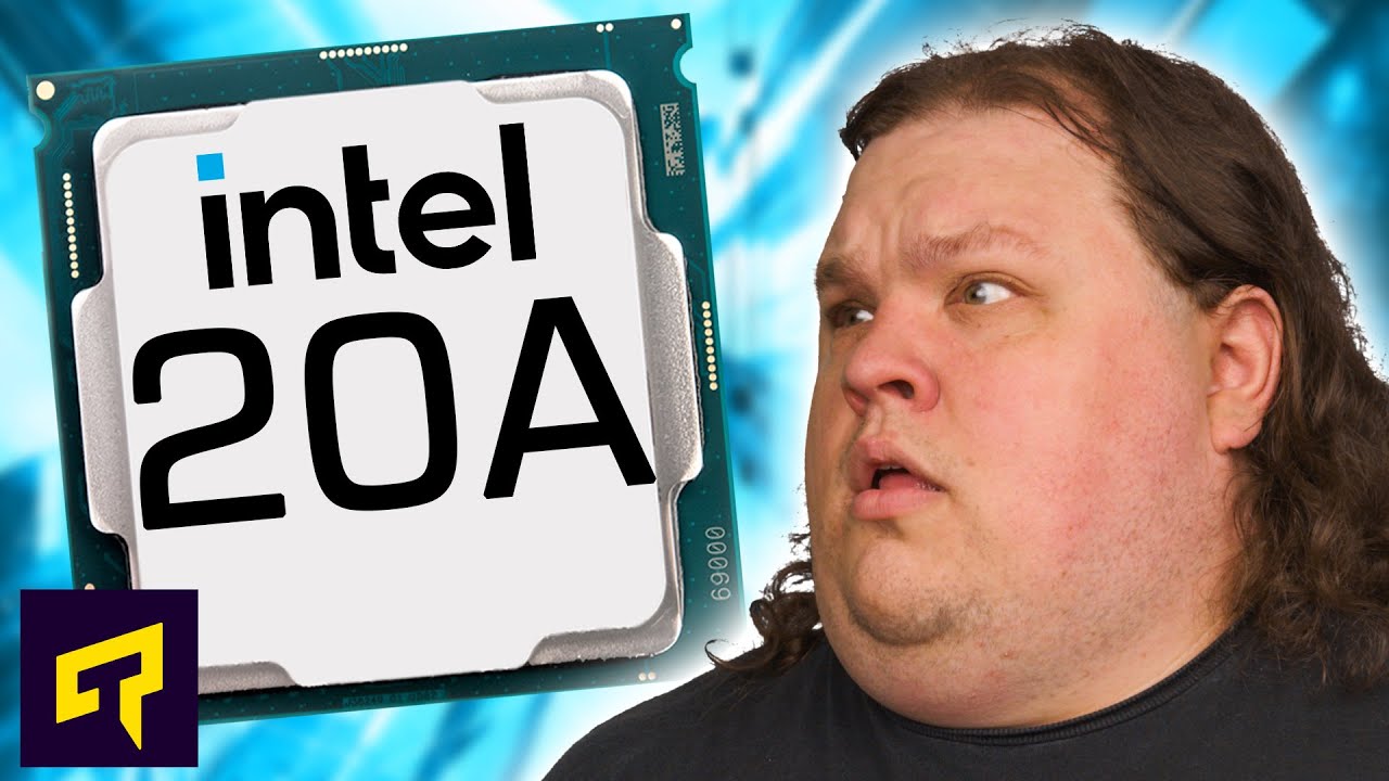
The video explains how the semiconductor industry has progressively shrunk transistor sizes from the 5 to 20 nanometer range, enabling powerful CPUs and compact devices, and why the industry is moving toward angstrom-based measurements as sizes fall below two nanometers. It highlights that measurements in integers lose meaning at extreme scales, since moving from one node to the next can be as impactful as large leaps in performance, yet the public labels may understate the real gains. The presenter then details Intel’s plan to adopt angstrom-based naming, with targets like 20a and 18 angstroms to follow, and explains that one silicon atom is roughly two angstroms in diameter, underscoring the approaching physical limits of silicon as a base material. To address these limits, the video describes architectural and process innovations such as gate-all-around transistors, which improve current control and allow stacking of transistors to cram more onto a chip. Extreme ultraviolet lithography (EUV) is another critical enabler, enabling smaller transistors to be etched into silicon, though Intel has faced supply and adoption challenges compared with competitors like Samsung and TSMC. The host clarifies that exact process node numbers are not standardized across companies, as different firms measure process nodes differently, and Intel’s roadmap uses non-nanometer/angstrom designations for upcoming nodes. Overall, the episode ties together material science, lithography technology, and strategic decisions shaping how future CPUs will be designed and manufactured, setting expectations for Intel to compete with peers in both high-performance and potentially contract-manufacturing markets while addressing the limits of conventional silicon technology.
Topics · science and technology · semiconductors · cpu architecture · chip manufacturing
Questions answered
- Why are angstroms being used instead of nanometers for CPUs at advanced nodes?
- Angstroms are being adopted because at extreme scales, traditional nanometer labels lose granularity and can be misleading; an angstrom-based naming can better reflect the very small sizes and the dramatic improvements in transistor density that occur with each generation.
- What architectural changes enable more transistors on a chip besides shrinking transistor size?
- Gate-all-around transistor designs improve current control and allow stacking of transistors, which increases transistor density without relying solely on smaller feature sizes.