Nvidia Wouldn't Send Me This $30,000 GPU - H200 Holy $H!T
0 up · 0 down · 0 ratings
Description
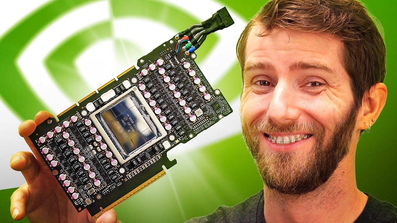
Get Grammarly today! grammarly.com Purchase a Valkyrie V-Lite AIO at: kont.ly kont.ly The H200 is an incredibly powerful generative AI and high-performance computing card that costs tens of thousands of dollars. So of course we tested it and tore it down. For uh, science.
Promos
Check out the Labs article: lttlabs.com Discuss on the forum: linustechtips.com ► GET OUR MERCH: lttstore.com ► GET EXCLUSIVE CONTENT ON FLOATPLANE: lmg.gg ► GET A VPN: piavpn.com ► SPONSORS, AFFILIATES, AND PARTNERS: lmg.gg Purchases made through some store links may provide some compensation to Linus Media Group. Affiliate links powered in part by affilimate.com Linus Sebastian is an investor in Framework Computer, Inc CHAPTERS --------------------------------------------------- 0:00 Intro 1:18 H200 NVL 2:22 Teardown 8:21 H200 vs Dual Epyc 9965 16:03 H200 vs RTX 5090 19:30 Benchmarks 21:20 Conclusion 22:51 Outro
Channels and socials
Check out Level1Techs: @Level1Techs
Nvidia would not send the hosts a test sample of the H200 NVL GPU, so they secured one and tore it down to understand what the $30,000 device is actually capable of. The video opens with a bold setup, situating the H200 as a massively powerful AI and HPC card with a 80 billion transistor die, HBM memory, and a colossal 4.8 terabytes per second bandwidth. The presenters explain the practical context that enterprise deployments may utilize hundreds or thousands of these GPUs, dwarfing consumer SKUs and highlighting how a single card fits into a much larger infrastructure. They then walk through the card’s physical design, shielding, and exotic memory architecture, emphasizing the dense die, vapor chamber cooling, and the direct memory interface that helps power efficiency. The teardown reveals an impressive but bewildering assembly: a large VRM on the card, six HBM stacks, and a cooling approach that relies on server-style airflow rather than a traditional fan, underscoring the engineering focus on efficiency and density rather than consumer gaming experiences. Throughout, the hosts connect architectural choices to real-world outcomes, noting that power draw is high (around 600 W) but that the memory bandwidth and stacking approach are key to AI workloads and training scenarios. In parallel, they compare the H200 to a dual AMD Epic 9965 server and to consumer GPUs like the RTX 5090, setting up a broader discussion about why enterprise-grade hardware can outperform consumer graphics in AI tasks and how that translates to cost of ownership and operating expenses in large-scale deployments. The discussion then pivots to practical benchmarks, where they run GPT-family workloads and other AI tests, using a 65 GB OpenAI OSS 120B model and a 141 GB VRAM-capacity busy setup, highlighting how context, prompt strategy, and fresh model loads affect throughput. They also juxtapose Blender rendering performance, showing that traditional CI workloads may still favor professional hardware in some scenarios, but AI workloads reveal a surprising tilt toward consumer-class GPUs in several tests. The lab-style benchmark section digs into model loading times, token throughput, and the impact of VRAM vs system RAM, illustrating how the H200’s design choices translate into real-world training and inference times. Finally, the video reflects on future hardware like the next-generation B200 or B300 and emphasizes that while the H200 is extraordinary, the technology landscape will continue to evolve rapidly, with enterprise features and efficiency continuing to drive the AI hardware race. The wrap-up touches on sponsorships and additional content, hinting at more deep-dive explorations and comparisons across the family of high-end accelerators, with a nod to ongoing AI benchmarking on the lab website and partner channels.
Topics · technology · hardware · ai · benchmarking · teardown · gpu · data-centers · computing
Questions answered
- What makes the Nvidia H200 NVL different from consumer GPUs?
- The H200 NVL uses a dense die with HBM stacks, a large VRM, and a vapor chamber cooling system designed for high efficiency and bandwidth, enabling large-scale AI workloads and training rather than consumer gaming performance.
- Why did Nvidia reportedly not send a test unit for review?
- The video implies Nvidia may reserve such enterprise-class hardware for large corporate deployments and that giving early access could involve complex configurations and licensing that are not suitable for a casual teardown.
- How does the H200 compare to the RTX 5090 in benchmarks shown?
- In the lab tests, the H200 showed varying results, sometimes outperforming in AI-specific tasks due to its memory architecture and scaling, but the RTX 5090 often remained highly competitive in consumer workloads like Blender rendering, highlighting the different design goals of each class of GPU.
- What is the practical takeaway for viewers considering such hardware?
- For most users the card represents a specialized, expensive solution aimed at enterprise AI workloads; for individuals, opportunities lie in understanding the architecture and tradeoffs, not in direct gaming performance.