You Didn’t Build your PC… This Did. - ASML Cymer Tour
0 up · 0 down · 0 ratings
Promos
Get unbiased breaking news and compare coverage at ground.news Use my link to download the app for free or subscribe to the Vantage plan for 30% off. Offer ends June 2nd and is only available through the Ground News website. Create your build at buildredux.com Building a computer is difficult and building a CPU is even tougher.. But building the machines that are used to make a CPU? It takes literally the most bonkers engineering and physics on the planet, and ASML were kind enough to show us how it all works. Discuss on the forum: linustechtips.com ► GET MERCH: lttstore.com ► LTX 2023 TICKETS AVAILABLE NOW: lmg.gg ► GET EXCLUSIVE CONTENT ON FLOATPLANE: lmg.gg ► SPONSORS, AFFILIATES, AND PARTNERS: lmg.gg ► EQUIPMENT WE USE TO FILM LTT: lmg.gg ► OUR WAN PODCAST GEAR: lmg.gg FOLLOW US --------------------------------------------------- Twitter: twitter.com Facebook: @LinusTech Instagram: @linustech TikTok: @linustech Twitch: twitch.tv MUSIC CREDIT --------------------------------------------------- Intro: Laszlo - Supernova Video Link: youtube.com iTunes Download Link: itunes.apple.com Artist Link: soundcloud.com Outro: Approaching Nirvana - Sugar High Video Link: youtube.com Listen on Spotify: spoti.fi Artist Link: youtube.com Intro animation by MBarek Abdelwassaa @mbarek_abdel Monitor And Keyboard by vadimmihalkevich / CC BY 4.0 geni.us Mechanical RGB Keyboard by BigBrotherECE / CC BY 4.0 geni.us Mouse Gamer free Model By Oscar Creativo / CC BY 4.0 geni.us CHAPTERS --------------------------------------------------- 0:00 Intro 0:50 How are transistors made? 3:08 Just blast tin with lasers 4:20 Getting suited up 6:46 Liquid tin delivery system 8:42 Droplet Generation Qualification 10:45 There are way more steps to lithography 12:24 ASML helps everyone! 14:16 Ground News 15:35 Outro
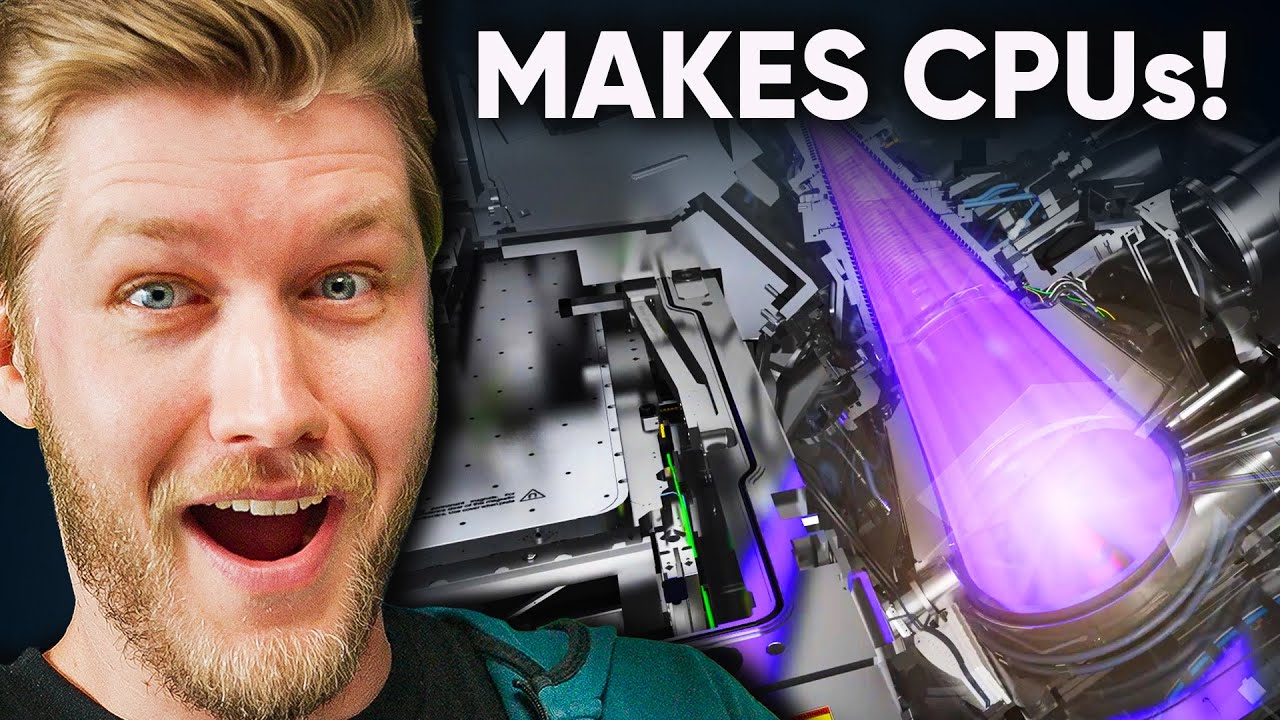
The video opens with LinusTechTips visiting ASML in San Diego to explore the extraordinary machinery that enables modern microprocessors. The host introduces the core challenge of making transistors at nanometer scales and explains that EUV lithography relies on a 13.5 nanometer ultraviolet light produced by a laser-driven tin plasma. A vivid comparison to an overhead projector helps lay a mental model for lithography, while the host emphasizes how each component of the system must be engineered to handle extreme precision and extreme power. We then dive into the droplet generation process, where tin is shaped and shot at high pressure to create the plasma essential for EUV light, and we see how the system uses multiple laser stages to amplify the light to the tens of kilowatts needed for production. The narrative continues with conversations about laser safety, isolation techniques, and the bespoke equipment that prevents reflections from damaging the laser chain, underscoring the sheer scale and risk-management involved in maintaining uptime. Finally, the video discusses the broader manufacturing context, including metrology, wafer alignment, and the pipeline from source to customer fabs, while also acknowledging the immense cost and production demands of keeping these machines running nonstop. The host wraps with glimpses of the future, noting high-NA EUV advancements and the likely path toward even smaller feature sizes, before thanking the ASML team and the Ground News sponsor. Overall the video blends engineering storytelling with hands-on visuals of a cutting-edge semiconductor toolchain, delivering a tutorial-like tour that connects the physics of EUV generation to the practicalities of operating a multi-hundred-million-dollar machine. Viewers gain a sense of how precision, safety, materials handling, and supply chain logistics converge in a facility designed to manufacture the chips powering contemporary devices. The pacing interleaves technical explanations with on-site demonstrations, creating a narrative arc from fundamental physics to real-world deployment. By spotlighting personnel and processes, the video also conveys the organizational complexity and expertise required to push the boundaries of lithography and semiconductor manufacturing.
Topics · science and technology · manufacturing · engineering · technology
Questions answered
- What makes EUV lithography different from previous lithography methods?
- EUV lithography uses extremely short wavelength light (13.5 nanometers) and specialized optics, including multilayer mirrors, to print incredibly small features. Unlike earlier deep UV approaches that relied on lenses and more traditional mirrors, EUV requires a laser-produced tin plasma and a carefully engineered light path to minimize absorption and reflection losses while maintaining nanometer-level alignment.
- Why is uptime so critical for ASML’s EUV machines?
- EUV machines are among the most expensive and central components in a fab, with costs around 150 to 200 million dollars each. Downtime halts production for the entire facility, so uptime targets are set very high (nearly 90% currently, aiming for 95% by 2025) and maintenance is meticulously planned to avoid costly losses.